Date: 15 September 2012
Higher-power and higher-beam-quality lasers continue to emerge on the marketplace, and industry continues to find new uses for them.In particular, glass processing has garnered much attention in recent years. Common tasks such as cutting, grooving, milling and drilling are routinely performed in various types of glass and with various types of lasers. More advanced processes such as annealing, welding and refractive index modification – for waveguide and diffractive optical element fabrication, for example – are also being explored. Markets and applications using such processes are quite varied, ranging from the routine to the exotic; and they will undoubtedly grow and diversify as industries discover more about what lasers can do in terms of noncontact structuring of glass.
Processing glass with lasers is not without challenge. The fact that glass is transparent to the most commonly available laser wavelengths requires that high peak intensities are generated to trigger a nonlinear absorption effect. With good beam quality, high pulse energies and short pulse durations, such high intensities can be generated in the glass with relatively long-focal-length lenses. This, combined with high pulse repetition frequencies of hundreds of kilohertz for high throughput, is helping to make laser glass processing a feasible solution for a growing number of industrial applications.
Laser technologies for glass
Various types of lasers are used for different types of glass machining tasks. For full-cutting long straight lines in thicker glasses, carbon dioxide (CO2) lasers are commonly used. In one approach, the focused laser beam heats the glass and is followed by a cooling gas or liquid, resulting in a straight-line fracture of the glass achieved at relatively high speeds – meter lengths can be cut in a matter of seconds. This approach, however, is not generally successful for thinner glasses much below about half a millimeter in thickness. In addition, any desire to cut curved contours cannot be addressed.
Compared with CO2 lasers, ultrashort-pulse (USP) lasers with picosecond and femtosecond pulse widths are at opposite ends of the spectrum in terms of cost per watt and technological complexity. But these lasers also are used for glass processing because they can machine various intricate shapes in glass with very high quality. The quality is excellent because nonlinear absorption phenomena allow small irradiation depths, resulting in controlled material removal and corresponding edge chipping dimensions down to 10 µm or less. However, for the same reason that good quality is achieved, the processing also is relatively slow, with centimeter-diameter holes in 1-mm-thick glass requiring minutes of drilling time. This technology is appropriate for value-added applications, in which the high cost and low throughput of the laser are acceptable because of the uniqueness of the result.
Besides CO2 and USP lasers, a third option for glass processing is the nanosecond-pulse, Q-switched diode-pumped solid state (DPSS) laser, which falls near the middle of the spectrum in terms of complexity and dollars per watt. Glass processing with such lasers inherits qualities of both the fast, crude CO2 tool and the slow, fine USP scalpel. Although the speed is lower than that of the straight-line CO2 laser cuts, the quality can be better – and what’s more, contoured shapes can be cut. Likewise, compared with USP laser processing, the edge chipping formed with nanosecond-time-scale pulses is larger – often several tens of microns – but the throughput can be significantly higher and at a much lower cost.
Markets for glass processing
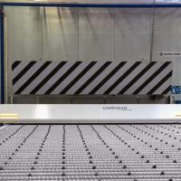
Various markets and industries currently benefit from laser glass processing. For example, in the fabrication of biomedical lab-on-chip devices, lasers are used to machine microgrooves, titration vias and even embedded waveguides for optical sensing. For such devices, short nanosecond-pulse Q-switched DPSS lasers can be used for high-quality, cost-efficient glass processing. One example application is fast subsurface micromarking of glass parts with a short nanosecond-pulse laser at the 355-nm wavelength. Figure 1 shows a variety of subsurface glass marks machined with just such a laser.
Figure 1. Nanosecond-pulse Q-switched DPSS lasers can produce high quality in glass processing. Here, various subsurface micromarkings in glass are made with a 355-nm, nanosecond-pulse Q-switched laser (Spectra-Physics’ Tristar series 355-nm 2- to 3-W lasers). Single-character marking times are as low as 10 ms.
These lasers offer good marking power of 2 W or more at a very reasonable cost; and with fast pulse trains at 50 to 100 kHz or more, typical write times of a few tens of milliseconds per character are achieved, translating to a marking capability of several tens of characters per second. Although the biomedical lab-on-chip market is relatively small, it likely will grow as medical-related industries continue to see large capital investments. Industrial-grade, high-throughput and high-quality lasers such as this can offer cost-effective solutions for the demands of high-volume production tasks.
A much larger market for glass processing is flat panel device (FPD) and touch sensor panel (TSP) manufacturing. Consumers worldwide continue to embrace and integrate smartphones and tablet devices into their lives, and this will no doubt drive a need for tools to manufacture ever-more complex shapes and structures in glass. The glass used for these devices is relatively thin and likely to get thinner. With the unveiling of various surface-strengthened glasses such as Corning Gorilla Glass and Schott Xensation – not to mention the likelihood of further innovation – glass thicknesses are expected to decrease sharply from the current standard of 0.3 to 1.1 mm to perhaps no more than several tens of microns.
Figure 2. Nanosecond-pulse Q-switched lasers can cut closed-shape geometric figures in strengthened glasses. Here, a 5-mm-diameter through hole has been cut in 1.1-mm-thick Gorilla Glass for smartphone production. Cutting time is ~15 s.
Although the need for glass processing in the FPD/TSP markets is large and growing, it is at the same time unclear exactly which laser technology can meet the quality and throughput demands. In some cases, nanosecond-pulse Q-switched lasers have been used to cut closed-shape geometric figures in such strengthened glasses (Figure 2). Compared with the previously highlighted marking application, power requirements are much higher; in this case, a Spectra-Physics Pulseo 355-20 laser system that delivers <20-ns pulse durations, pulse energies above 200 µJ and 100-kHz repetition rates was used.
The high laser power results in reasonable throughput; however, the as-cut edge quality can be good but imperfect. Depending on the exact details of an application’s demands, some postprocessing steps such as chamfering/polishing may be required. In some applications, these added steps are undesirable. Perhaps a more finesse-oriented laser – for example, a high-power and high-pulse-repetition-frequency femtosecond-pulse laser – could be the right solution. Indeed, this class of laser offers high-quality structuring of glass materials with excellent surface and edge quality for precision processing (Figure 3).
Figure 3. A high-power, high-pulse-repetition-frequency femtosecond-pulse laser offers structuring of glass materials with good surface and edge quality. Here, 3-D glass structuring has been performed with a Spectra-Physics High Q femtosecond laser.
Glass processing for PV solar panels
Glass also is used extensively in thin-film photovoltaic (TFPV) manufacturing. With up to meter-size sheets of 1- to 3-mm-thick glass as a substrate, solar panels are produced with a variety of solar absorber materials, such as amorphous silicon (a-Si), cadmium telluride (CdTe) and copper indium gallium (di)selenide (CIGS). A well-known success story for Q-switched DPSS lasers in TFPV manufacturing is in scribing thin films of material – referred to as P1, P2 and P3 scribing – to create the panels’ monolithic serial interconnection architecture. But a typical TFPV panel is >99 percent glass by composition (before module packaging), so it would seem logical that laser glass processing could have potential somewhere along the production line.
Such an opportunity does arise in the final packaging of some TFPV panels if the same glass substrate on which the photovoltaic device is built becomes part of the rear side of the encapsulation package. When the panel is fully sealed – which includes metal framing around the perimeter – a through hole in this glass is needed to access the device’s electrical contacts.
Laser processing offers advantages for fabricating these conduit through-vias. Unlike mechanical drilling, the laser enables a noncontact process, which means low or no vibration is generated that can potentially weaken the devices’ thin films. Also, laser cutting of glass can be done as a completely dry process, which is important for thin-film materials such as the moisture-sensitive solar absorber layer.
Processing challenges for glass
Laser processing of glass in general is a fairly delicate operation because care must be taken to avoid excessive melting, chipping and cracking. Achieving the proper quality and throughput compromise requires a significant process development effort. This is particularly true when a higher-power laser is used for processing. The higher laser power enables faster processing, but it also increases the thermal loading on the glass, which can result in melting, cracking and even invisible weakening of the glass in the form of residual stress, any of which could cause product failure in the field.
To achieve proper thermal management in the glass, equipment and methods for focusing and scanning the laser beam must be carefully selected. One approach uses a high-speed two- or three-axis scanning galvanometer system with a flat-field f-Theta objective, which allows fast scanning of a tightly focused laser beam over a stationary glass plate. Today’s galvo scanner products allow speeds on the order of meters per second to be generated with relatively small scanning dimensions, down to 1 to 2 mm. Such rapid motion of the focused laser spot goes a long way toward minimizing heat buildup in the glass. Very thin glass can be cut with single or multiple overlapping scans of the focused beam. As glass thicknesses increase to the range of hundreds of microns, however, the laser cutting process becomes self-limiting. In this case, multiple adjacent beam scans are required to widen the kerf, facilitating debris removal and, ultimately, full cut-through of the thick glass. For still thicker glasses, it becomes necessary to translate the focused beam along the Z-axis through the bulk of the glass. At this point, the laser “cutting” process has clearly transformed into a 3-D laser milling process.
When applied to thin-film photovoltaic panel glass via drilling, the equipment and techniques detailed above result in quality through holes drilled in a matter of seconds for the requisite diameters of ~4 to 6 mm. The image in Figure 4 shows sample cross sections of cutouts generated with the Spectra-Physics Pulseo 532-34 laser system on 1-, 2- and 3-mm-thick glass substrates. Rated for 34-W output at 120-kHz pulse repetition frequency (PRF), the laser outputs >350 µJ at 100-kHz PRF; the combination of high pulse energy and fast pulse output enables rapid processing. And the <30-ns pulse duration allows controlled heat input into the material.
Figure 4. Quality through holes have been drilled in mere seconds for the requisite diameters of ~4 to 6 mm. Now laser-drilled holes in 1-, 2- and 3-mm-thick glass substrates can be of high quality as well, as shown here.
The cross-section cutaway of the holes shows near-vertical sidewalls of the cut and a fine, granular sidewall texture. The holes were processed in two stages, with the laser beam first incident upon one surface of the glass (stage 1) and next upon the opposite surface (stage 2). It can be demonstrated that such a processing strategy offers both quality and throughput advantages as compared with processing from just one side of the glass.
To improve throughput by reducing the volume of glass that must be removed, it is helpful to use two laser beams (either split from a single laser or from two lasers) to simultaneously or serially drill on opposite glass surfaces. Compared with the case of a single laser beam on a single side of glass, a significant reduction in the volume of material to ablate is achieved (Figure 5). Furthermore, as Figure 5 illustrates, two-side processing can reduce the overall taper of the hole as well because the difference between the outer and inner cutting diameters is halved.
Figure 5. Schematic illustration of laser-milled through hole shows how quality (taper) and throughput can be improved by processing on both surfaces of the glass.
Calculations show that only one-quarter of the volume need be removed for an ideal two-sided process. This equates to 4-times throughput improvement if two laser beams are processing simultaneously.
In laboratory testing, actual demonstrated throughput improvement is in the range of 3 to 3.5 times. If, instead, a single laser is used and the beam is rapidly switched to the second surface after processing the first, the advantage is halved, resulting in 1.5- to 1.75-times throughput improvement.
Glass processing configurations
There are three processing configurations to consider, each with an associated process throughput:
1. One laser that processes from one surface.
2. One laser that processes from two surfaces.
3. Two lasers that process two surfaces.
For 5-mm-diameter holes similar to those in Figure 3, Figure 6 summarizes the drilling times for each of these three process approaches, clearly demonstrating that significant throughput improvement is gained with processing configurations 2 and 3.
Time, in Seconds, to Cut 5-mm-Diameter Hole in Various Glass Thicknesses
Process Type
1-mm Thick
2-mm Thick
3-mm Thick
One Laser, One Surface
10.2
31.4
60.6
One Laser, Two Surfaces
6.2
18.5
36.4
Two Lasers, Two Surfaces
3.1
9.2
18.2
Figure 6. Drill times for 5-mm-diameter holes in 1-, 2- and 3-mm-thick glasses using various processing approaches. Using two lasers triples the throughput. Courtesy of Spectra-Physics.
The challenges of integrating two lasers for simultaneous processing of both surfaces of a glass plate are not trivial, and configuring a single laser to process from both sides is only slightly less complex. But considering the throughput improvements that can be realized, it may be a worthwhile challenge to undertake in many cases.
Meet the author
Jim Bovatsek is applications lab manager at Spectra-Physics in Santa Clara, Calif.; email: jim.bovatsek@spectra-physics.com. Dr. Rajesh S. Patel is director of strategic marketing, also in Santa Clara; email: raj.patel@spectra-physics.com.


Add new comment