Date: 18 September 2015
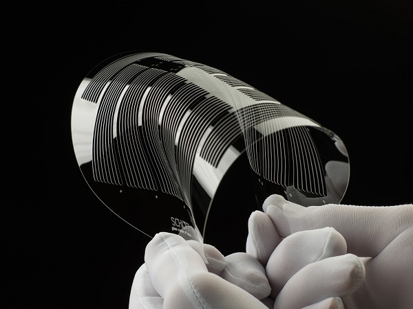
Thanks to its well-adapted thermal expansion behavior, its excellent flatness and process robustness, it is widely recognized as a standard material for MEMS processes such as anodic bonding.The high-performance material now also allows new forms of de-bonding. Laser de-bonding through a glass carrier wafer made of BOROFLOAT® glass is possible thanks to deep UV light transmission at the relevant laser wavelength range. This allows for the production of larger and thinner silicon wafers in a stable production process.
The constant trend towards smaller, more lightweight devices with 3D design architecture calls for ultra-thin silicon wafers with very high flatness levels. In addition, this quickly growing market demands higher yield rates, making larger and thinner wafers necessary. To reliably product such wafers, process stability becomes increasingly important. The temporary bonding of a silicon wafer to a carrier wafer is a necessary step during silicon wafer thinning. The quality of a carrier wafer is determined by its ability to allow for fast processing and de-bonding times and to achieve a default-free surface cleanliness of the silicon wafer..jpg)
„The reason that we use SCHOTT BOROFLOAT® glass is product performance and incredible service and technical support. At the moment I can’t imagine anything that SCHOTT needs to do better than those three things,” says Kevin Brolsma, President of Alpha Precision, Inc. Photo: SCHOTT.
Laser de-bonding through glass carrier wafers currently offers the fastest de-bonding time as well as a good price-performance-ratio. Deep UV light transmission at the relevant laser wavelength range is crucial for the principal feasibility and efficiency of this type of wafer de-bonding. SCHOTT’s BOROFLOAT® glass offers the necessary optical properties to support laser de-bonding. “The laser-activated release will be achieved through irradiation using a high power excimer laser at a fairly low wavelength of 248 nm or 308 nm. Extra-low iron BOROFLOAT® glass of desirable 0.5 mm carrier thickness shows over 90 % transmission at 308 nm and still over 35 % for 248 nm, thus significantly outperforming other thin flat glasses,” said Thomas Kloss, Senior Innovation & Product Manager for BOROFLOAT® at SCHOTT in Jena.
BOROFLOAT® also well-suited substrate for anodic bonding
Anodic bonding is widely used to combine silicon wafers with borosilicate glass to cap MEMS, other electronic and optical parts or to seal microfluidic devices. A perfect match between the two substrates is essential for good bonding behavior. “BOROFLOAT® glass offers the unique thermal, mechanical and chemical properties needed to meet the requirements for gap-free and long-lasting material bonds”, stated Kloss.
The thermal expansion behavior of BOROFLOAT® glass over a wide temperature range compares to that of silicon and thus makes it ideal for anodic bonding processes. Furthermore, many wafers require microstructures created via ultrasonic drilling, powder blasting or a combination of photolithography and dry etching. The high abrasion resistance of BOROFLOAT® glass compared to other alternative substrates allows for the necessary mechanical strength and stability required for microstructuring.
In addition, BOROFLOAT® glass also offers high chemical resistance which is relevant when the wafers are exposed to chemicals throughout highly sophisticated etching and chemical mechanical planarization (CMP) processes. Even mask-based chemical etching technologies can be applied to SCHOTT’s borosilicate wafers in order to create high definition surface channels.
For more information visit: www.schott.com/borofloat/wafer
www.youtube.com/watch?v=A8U2uWrJHi0&list=PL18D52AF21B34E561
BOROFLOAT® is a registered trademark of SCHOTT AG.
SCHOTT is a leading international technology group in the areas of specialty glass and glass-ceramics. The company has more than 130 years of outstanding development, materials and technology expertise and offers a broad portfolio of high-quality products. SCHOTT is an innovative enabler for many industries, including the home appliance, pharmaceutical, electronics, optics, automotive and aviation industries. SCHOTT strives to play an important part of everyone’s life and is committed to innovation and sustainable success. The group maintains a global presence with production sites and sales offices in 35 countries. With its workforce of approximately 15,400 employees, sales of 1.87 billion euros were generated in fiscal year 2013/2014. The parent company, SCHOTT AG, has its headquarters in Mainz (Germany) and is solely owned by the Carl Zeiss Foundation. As a foundation company, SCHOTT assumes special responsibility for its employees, society and the environment. www.schott.com


Add new comment