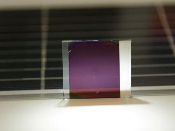
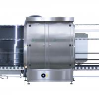
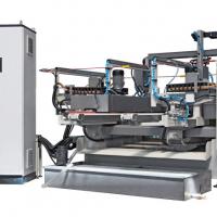
The construction of a solar production plant, located near Varese, northern Italy, expected to produce 15 MW/year, will also be reported. This plant, based on CdTe thin film deposition onto 0,6 x 1.2 square meter glass modules, is being built with the scientific support of Parma University.
The massive use of photovoltaic modules has so far been limited by the high cost when compared to that of electrical energy obtained from conventional energy sources. In order to lower the cost, several materials have been studied and thin film modules have been developed as an alternative to crystalline silicon. Thin films have the advantage that only a few microns of material are needed and that the modules can be monolithic which means that the contacts between the single cells inside the modules are made during the process by using automated laser scribing and material deposition one after each other. This, in prospective, can lower the cost below 0,5 USD/W which is competitive with the cost of electrical energy obtained from conventional sources.
THIN FILMS
Amorphous silicon
Three kinds of thin films are now commercially available, namely: a-Si, CdTe/CdS and CuInGaSe2/CdS. Amorphous Silicon (a-Si) has covered a large part of the market up to now but polycrystalline thin films are growing fast since they are more efficient and more stable. Polycrystalline thin film solar cells have made big progress during the last 20 years. An efficiency close to 20 per cent[1] has been reached for CIGS (CuInxGa1-xSe2) and 16.5 per cent[2] for CdTe. Several solar production plants with the aim of producing large size modules of both materials have been built in the last years. Production capacity, at least for one of these materials, namely CdTe, is getting close to 1 GW/year. Considering that modules of these materials are produced by depositing thin films on glass, a square meter of glass can give 100 Wp of solar power if an efficiency of 10 per cent is obtained. In the next 12 years a production as high as 100 GW/year is foreseen. This means that 109 square meters of glass are required. The need for such a large amount of glass has pushed several glassworks to make commercial agreements with solar plants.
CIGS
This material exhibits the highest efficiency with the composition of CuIn0.75Ga0.25Se2 at which a forbidden gap of 1.2 eV corresponds. Being a mixture of CuInSe2 (forbidden gap EG = 1.1 eV) and CuGaSe2 (forbidden gap EG = 1.7 eV), by changing its composition, it can exhibit any forbidden gap between 1.1 and 1.7 eV. Since the maximum theoretical efficiency lies generally at 1.5 eV, one can change the composition to obtain such a forbidden gap. But, by increasing the Ga content above 30 per cent, both diffusion length and lifetime of minority carries decrease and this is the reason why 25 per cent Ga gives the highest efficiency.

Figure 1 - Schematic of the CuInGaSe2/CdS solar cell structure

Figure 2 - Four sources deposition chamber
The structure of this cell is shown in Figure 1. As a substrate, soda-lime glass is generally used even though substrates such as molybdenum or steel foils and polymers have been used in order to obtain flexible solar cells. One important thing to be taken into consideration is that soda-lime glass substrates give the best results since some Na diffuses through the Mo layer into the CuInGaSe2 films, that are grown at 500°C or more close to the glass softening point. Na diffusion improves the crystallinity of the material and dopes ρ-type the film. When other substrates, different from soda-lime glass are used, Na is added by depositing a thin layer of NaF on top of CuInGaSe2 and then annealing at 500°C. The first problem that is encountered in the fabrication of CIGS solar cells in the preparation of Mo layer due to the large thermal and lattice mismatch between Mo and glass and CIGS and Mo. Some researchers resolved such a problem by depositing three or more Mo layers one on top of each other with different deposition rates and different Ar pressures in the sputtering chamber. We resolved this problem by simply depositing the Mo layer by D.C. sputtering at room temperature and then by depositing a 200 nm thick layer of In2Se3 on top of it followed by 20 nm of Cu and then annealing at 400°C for half an hour. During the annealing the stress in the Mo film is entirely eliminated and the substrates is ready for the following deposition of CuInGaSe2 by a multi-source deposition system (Figure 2) that is by using four different evaporation sources for the four elements that compose the material.
Generally a Cu-rich material is deposited at the beginning and then a Cu-poor material is deposited at the end. This is carried out in order to avoid the formation of a CuxSe phase at the surface which, being unstable, can lead to Cu diffusion through the junction, irreversibly damaging the cell. The CuInGaSe2 layer is the most critical part of the cell, since both CdS and ZnO or ZnO(Al) can easily deposited by simple techniques. However, even though multisource deposition gives the best results, it is not suitable for large scale application, since it cannot guarantee the same stoichiometry over a large area. A different approach is now being pursued, consisting in the deposition of the elements one on top of each other, followed by an annealing at high temperature and a subsequent selenization. However, as in In and Ga are low melting point elements, a deviation from the right stoichiometry could be present in some zones of the layer if the substrates temperature is not maintained perfectly uniform in every point. In out laboratory we substituted In with In2Se3 and added Ga by using an alloy Cu-Ga that is solid also at high temperatures, the CuInGaSe2 film is prepared in the following way.
After the stress of Mo is removed by following the procedure described previously, 1 µm of In2Se3 is deposited by an electron gun, In2Se2 is then covered by 100 nm of Cu and annealed for half an hour at at substrate temperature of 400°C. This mixed layer (precursor) is put in a vacuum chamber where it is exposed to Se vapour for half an hour at 520 °C substrate temperature. In this way a stoichiometric CuInSe2 film is obtained. In order to enrich the material in Ga a subsequent deposition of Cu and Ga is carried out on top of the CuInSe2 film by electron gun and then selenized at a 520°C substrate temperature.
This method permits to obtain stoichometric CIGS films over large areas with an efficiency of 15 per cent. In order to further render this procedure scalable over large areas all the materials should be deposited by sputtering and this is the road which we are now following. Even though the problems connected with the large area production of CIGS modules are still not completely resolved, there are at least 12 companies that are now producing or are close to going into production with this material (Table 1)[3].
CdTe
CdTe exhibits very good characteristics as a thin film photovoltaic material. It has a forbidden gap of 1.45 eV, close to the theoretical maximum of photovoltaic solar energy conversion. Its gap is direct that means that only a few microns of the material are needed for the absorption of 90 per cent of solar light. It exhibits a very simple phase diagram and it grows stoichiometrically at a substrate temperature greater than 300°C in vacuum since excess elements, due to their high vapour pressure, reevaporate. The only drawback is that, when it is prepared as a thin film, it grows polycrystalline and exhibits grain boundaries. For this reason it cannot be doped since foreign impurities segregate into grain boundaries.
Fortunately, when CdTe is deposited at high temperatures, namely 500°C, it grows naturally greek ρ-type with a number of carriers greater than 1014 cm-3. Furthermore, defects in grain boundaries are, for the most part, removed if CdTe is annealed for 10-20 minutes at 400°C in presence of Chlorine. CdTe is considered the easiest material to be scaled-up since scalable and high deposition rate techniques such as Close-Spaced Sublimation (CSS) and sputtering are used to produce CdTe modules. For this reason, many companies have been founded during the last few years with the aim of producing CdTe modules (Table 2).
Among these companies, only First Solar and Antec Solar are producing at this moment. However, First Solar is increasing its production capacity very fast and has announced that it is closed to producing 1GW/year.


Cells of this type are composed of four layers as shown in Figure 3, namely front contact, CdS, CdTe and back contact. Both front and back contacts are composed of two sub-layers. Differently from CIGS, CdTe solar cells are of the superstrate type, that is, the light enters from the bottom glass, goes through the transparent front contact and the CdS and finally arrives to the CdTe where it creates the pairs of electronholes. All the layers that compose the cell have been prepared by using a proprietary process. The front contact is made by depositing 400nm of ITO (90 per cent In2O3+10 per cent SnO2) by sputtering. This layer exhibits a transparency greater than 85 per cent and a sheet resistance of 5 cm2. The ITO is covered by 150nm of intrinsic ZnO that is carried out by D.C. reactive sputtering in an atmosphere of Ar containing 20 per cent of O2 using a Zn target.
The resistivity of ZnO is about 103 .cm. The role of the ZnO layer is both to hinder the In diffusion from ITO and to separate CdS from the high conducting ITO in order to limit the effect of eventual pinholes that could be present in CdS, since the material has to be very thin , in the order of 80nm. CdS is deposited at a 250°C substrate temperature by R.F. (Radiofrequency) sputtering in an Ar atmosphere five per cent of CHF3.
The presence of F in the sputtering discharge, due to the substrate bombardment by negative F ions, permits the growth of a stoichiometric film with better optical characteristics such as immproved transparency and a sharper absorption edge.

Figure 3 - Schematic of the CdTe/CdS solar cell structure
CdTe is deposited by Closed Space Sublimation (CSS) at a substrate temperature of 500°C in an Ar atmosphere. Closed Space Sublimation means that substrate and source are very close to each other and deposition is carried out in an atmosphere containing an inert gas such as Ar. This technique gives for very high deposition rates in the order of several micron/min. For this reason it is suitable for large scale production. CdTe, in order to exhibit high efficiency, needs to be treated at 400°C in an atmosphere containing Cl. Generally, CdCl2, deposited on CdTe by evaporation or by dipping in a solution contained CdCl2, is used. In our case, we used a mixture of Ar and hydrofluorocarbon (HCF2Cl) avoiding the step of CdCl2 deposition[4]. After the treatment, CdTe is transferred into a vacuum chamber maintaining the temperature at 400°C in order to remove any residual CdCl2 that could form on the CdTe surface by evaporation.
Cl-treatment has the effect of removing the defects from the grain boundaries through a recrystallization process. In fact, during the treatment, small grains go into a vapour phase and, re-solidifying, contribute in increasing the size of large grains. The following reaction is supposed to take place during the Cl-treatment:
2Cl2 (gas) + CdTe (sol) > CdCl2 (gas) + TeCl2 (gas) > CdTe (sol) + 2Cl2 (gas)
HCF2Cl is an inert and non-dangerous gas at room temperature. However, it is considered an ozone belt depleting agent and must be recovered when used in industrial production.
The most critical part in CdTe solar cells is probably the back contact. Also in this case we developed our own recipe[5]. Generally, a good contact in CdTe is made by using some copper that, reacting with a Te-rich surface can form the phase CuxTe.
In order for this phase to be stable, x has to be ≤1.4. For this reason, most people use an amount of copper as thin as 2nm. If a phase with x larger than 1.4 is formed, copper that is not strictly bound diffuses through the grain boundaries of the CdTe damaging the cell.
Our recipe is quite simple: we put a buffer of As2Te3 between CdTe and Cu. If Cu is deposited at a substrate temperature of 200°C, it replaces As forming CuxTe. Depending on the As2Te3 thickness, As2Te3 can stop a large amount of Cu such as 20nm or more. Solar cells made with this contact resulted to be stable and efficient. Efficiencies close to 16 per cent have been measured in our laboratory. Five patents have been deposited to cover all parts of this process.
Having simplified the process, we designed an in-line system suitable to produce 15MW/yr, that means, working in three shifts, one 0.6x1.2m2 module every two minutes.

Figure 5 - Comparison between the old and the new in-line process
The simplified in-line system is shown in Figure 5 together with an old-line system. In the new process, two parts are eliminated, the chamber for the deposition of CdCl2 and the chemical bath for CdTe etching which is normally used to create a Te-rich surface before making the back contact.
In the in-line system, a three to four millimetre thick glass with a size of 0.6 x 1.2 sqare metres is introduced into a washing machine and then into a sputtering system where the glass is covered by the front contact that is ITO+ZnO. After this, the front contact is eliminated by a laser scribing along very narrow lines (50-100 µm) parallel one to each other and one centimetre apart in order to obtain strips one centimetre wide and as long as one dimension of the glass separated one from each other. The glass then enters a sputtering machine where CdS is deposited. In sequence, after increasing the glass temperature to 500°C, CdTe is deposited by a modified Closed Space Sublimation (CdTe vapor is transported in a tube and then deposited onto CdS from top to bottom) (Figure 4). After CdTe deposition a second laser scribing is carried out along lines parallel and very close to the first lines. This scribing must be carried out in order to eliminate CdS and CdTe but without touching the front contact.
The last section is represented by the back contact where As2Te3, Cu and Mo are deposited in sequence by sputtering. Finally, a third laser scribing is carried out close to the previous one in order to eliminate the back contact where it can short circuit the cells and, at the end, a monolithic module where the strips are put in series one to each other is obtained.
This in-line system is now under construction and will be ready in June 2009. One third of the line can be seen in Figure 6. The cost of the solar plant is around EUR 40 million. In order to build the plant, a new company, whose name is Arendi, has been founded. Participants of the company are: EuroEnergy Group (Marcegaglia), IFIS bank of Venice, Alchimia SpA (Marina Salomon), Studio Galli Ingegneria and Solar System and Equipments (SSE) that gives technical and scientific support through the University of Parma.
The Environment Ministry, through the Regione Lombardia, has contributed in the realization of this project with EUR 9 million.
CONCLUSIONS
The photovoltaic market is expanding year after year. Up to now, starting from the year 2002, there has been an increase of 40 per cent per year. Even though most of the present photovoltaic market is based on crystalline and polycrystalline Si, thin films are acquiring and important role and, in the near future, since their cost is decreasing with the cost of Si-modules is stable, they are destined to became the predominant part of the market. Among thin film materials, CIGS and CdTe are the most promosing, since they have shown good efficiencies and stability.
Moreover, there is still room to develop the technology of these materials further and an increase in module efficiency and a decrease in production cost are foreseen in the near future. Since both these materials mainly use glass as a substrate, the glass industry will play an important role for the massive expansion of these thin film photovoltaic modules.
ACKNOWLEDGMENTS
We finish to thank the Italian Ministry of the Environment, Land and Sea for partially supporting this work.
N. Romeo, University of Parma, INFM-PHYSICS DEPARTMENT, PARMA, ITALY
A. Bosio, University of Verona, PHYSICS DEPARTMENT, VERONA, ITALY
S. Mazzamuto, SOLAR SYSTEM AND EQUIPMENT S.R.L. (SSE), PISA, ITALY
REFERENCES
[1] I. Repins, M.A. Contreras, B. Egaas, C. DeHart, J. Scharf, C. L. Perkins, B. To, R. Noufi, National Renewable Energy Lab, MS 3219, CO, USA. Progress in Photovoltaics (2008), 16(3), 235-239.
[2] X. Wu, Solar Energy, 77 (2004) 813-814
[3] H.S. Ullal and B. Von Roeden, Proc. 22nd Europen Photovoltaic Solar Energy Conf., 3-7 September 2007, Milan, Italy, pp. 1926-1929.
[4] N. Romeo, A. Bosio, A. Romeo, S. Mazzamuto, Proc. 21st European Photovoltaic Solar Energy Conf., 4-8 September 2006, Dresden, Germany, pp. 1857-1860.
[5] N. Romeo, A Bosio, S. Mazzamuto, A. Romeo, L. Vaillant-Roca, Proc. 22nd European Photovoltaic Solar Energy Conf., 3-7 September 2007, Milan, Italy, pp. 1919-1921.
PAPER PRESENTED AT THE XX111 A.T.I.V. INTERNATIONAL CONFERENCE “ADDING VALUE TO GLASS”, PARMA, NOVEMBER 2008
XXIV A.T.I.V. CONFERENCE
59TH NGF ANNUAL MEETING
FINAL PROGRAM

